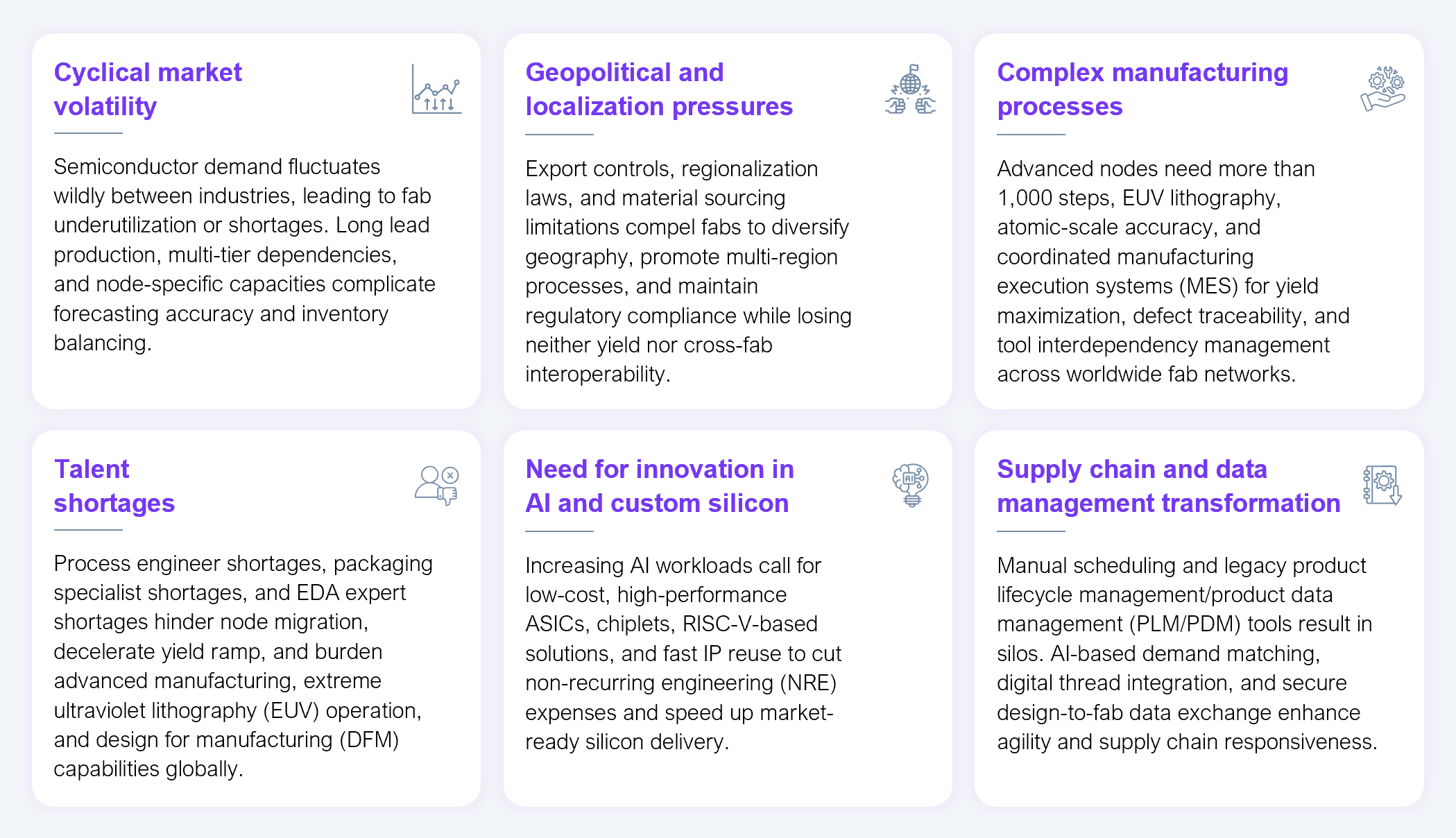
Semiconductor enterprises are under siege from geopolitical flashpoints, volatile demand curves, and brutal talent shortages. At the same time, they’re expected to deliver edge AI silicon in record time. Survival no longer hinges on scaling fabs, but on how fast they can master complexity, automate design cycles, and turn geopolitical risk into a strategic advantage. These challenges aren’t just obstacles; they’re the defining battlegrounds for the next generation of chip leaders (see Exhibit 1).
Source: HFS Research, 2025
The pandemic-driven chip shortage highlighted the fragility of global supply chains. Automotive leaders such as Ford and General Motors had to halt production, costing the industry over $200 billion in lost revenue. In 2025, the rising complexity arising from multi-tier dependencies, long lead times, and advanced node constraints has made volatility inevitable. The solution: deploy AI-driven demand forecasting, co-create inventory strategies with customers, and build highly flexible production models, turning disruption into a competitive differentiator.
For instance, Samsung uses AI-driven forecasting to simulate demand scenarios and dynamically adjust wafer starts, cutting excess inventory by nearly 15%. TSMC integrates machine learning into its logistics systems to predict component bottlenecks and reroute supplies in real time. Intel’s supply chain AI lab applies predictive analytics to identify disruptions weeks in advance, improving on-time delivery rates by 30%.
Geopolitical moves such as the US-China tech rivalry, the European Chips Act, and India’s $10 billion incentive program are reshaping global supply chains. To maintain yield and consistency across regions, manufacturers are investing in digital twins to simulate and synchronize fab operations, standardize process platforms to unify workflows, and develop compliance-first models to keep pace with the evolving regulations. Intel and TSMC are already using these tools to replicate quality across multi-region fabs. Such investments are turning geopolitical complexity into a competitive advantage, yielding resilient, globally aligned semiconductor ecosystems.
The industry still depends on specialized expertise in areas such as electronic design automation (EDA), packaging, and extreme ultraviolet (EUV) operations. Talent shortage is slowing node migrations globally. The U.S. CHIPS Act underscored this, highlighting the need for 90,000 new skilled workers by 2030.
Some leaders are responding to this; for instance, Intel’s partnerships with Arizona State University and TSMC’s training programs with Taiwanese universities show how academia-industry pipelines can scale talent. To turn such collaborations into real capability, enterprises must go beyond traditional training programs. Pairing academic partnerships with global reskilling initiatives enables continuous development of specialized talent rather than competing for scarce expertise. Embedding AI-assisted design tools into engineering workflows further accelerates this shift, automating routine design tasks, shortening verification cycles, and encouraging engineers to focus on higher-value innovation. Such efforts create a sustainable, adaptive talent ecosystem that keeps node migration and innovation on track.
At advanced nodes like 3nm, chipmaking involves more than 1,000 steps where a single defect can cascade across global fab networks. Scaling requires automation, AI-driven process control, and modular MES for seamless data exchange across sites. To scale effectively, semiconductor enterprises need more than incremental improvements; they need systems that can sense, adapt, and learn across sites in real time. That’s where automation, AI-driven process control, and modular MES architectures come together. A connected MES enables seamless data exchange between the wafer start and final testing stages, enabling enterprises to detect anomalies early, replicate best practices instantly, and keep global operations synchronized.
Samsung’s Smart MES, a core component of the massive automation at its Pyeongtaek mega-fabs in South Korea, and Intel’s modular MES upgrades for global foundries are prime examples of such implementations. These efforts resulted in increased yield, consistency, and customer trust while addressing complexity at scale.
The exploding AI demand is pushing semiconductor firms to deliver low-cost, high-performance custom silicon faster. Chiplets, RISC-V designs, and reusable IP are essential for accelerating development and reducing non-recurring engineering (NRE) costs. Leaders are already moving; for instance, NVIDIA uses AI-driven EDA to optimize graphics processing unit (GPU) design, while Google’s tensor processing unit (TPU) teams leverage open-source RISC-V and AI-assisted workflows to shrink design cycles. These examples show that AI automation and open architecture are no longer optional; they’re the levers that define the next generation of semiconductor leaders. The real question isn’t whether to adopt them, but how fast these capabilities can be built.
Legacy product lifecycle management (PLM) and product data management (PDM) silos are bottlenecks that slow the entire value chain at a time when agility is critical. As product complexity increases and demand cycles tighten, chipmakers need AI-driven demand matching, digital thread integration, and secure design-to-fab data exchange to remain agile. These capabilities enable end-to-end visibility, help anticipate demand shifts, and adjust production in real time, ensuring global consistency.
For instance, Siemens’ digital thread solutions at GlobalFoundries and Cadence’s cloud-based PLM integrations showed how connecting design, manufacturing, and logistics can transform operations. This resulted in a predictive, data-driven supply chain that turns volatility into resilience and disruption into a competitive advantage.
Chip leaders are increasingly seeing their firms at a crossroads where volatility, complexity, and innovation intersect. To navigate this environment, strike a balance between short-term risk and long-term innovation, invest in AI-resilient, multi-region operations and digital supply chains, and close the talent gap through global partnerships.
Register now for immediate access of HFS' research, data and forward looking trends.
Get StartedIf you don't have an account, Register here |
Register now for immediate access of HFS' research, data and forward looking trends.
Get Started