Semiconductor chips power every business, but the supply chain faces geopolitical challenges. Chip design, validation, and verification are essential for silicon self-sufficiency. Verification is the most labor-intensive and risk-prone stage, and it’s the largest cost component in chip development. The design process is stuck in manual mode—and that’s the problem. Seventy-five percent (75%) of application-specific chip projects are behind schedule, only 14% are resulting in first silicon success, and costs shot up in 2024, according to the Siemens EDA/Wilson Research Group/DVCon study findings. Chip designers and manufacturers should embed artificial-intelligence-driven validation and verification into the design process to ensure on-time, error-free, and within-budget manufacture and market delivery.
The DVCon India 2025 conference, held in Bangalore on September 10–11, provided a valuable opportunity to explore the integration of artificial intelligence (AI) into chip validation and verification.
Jean-Marie Brunet, Vice President and General Manager, Siemens Digital Industries Software, set the context with his first-day keynote address on “software-defined hardware design” and its reliance on AI and intelligent verification. “Software is the ultimate differentiator, and purpose-built silicon has become the competitive edge for every industry,” says Jean-Marie.
AI has become the foundation for the next generation of semiconductor design and verification. Chip designers relying on humans should realize that we have reached the limits of human cognition in this complex industry, and AI-assisted processes are the way forward.
Global semiconductor sales grew double digits in 2024, reaching $628 billion, and the Semiconductor Industry Association expects the trend to continue. The growth was spurred by increasing demand from the automotive, data center, telecommunications, and consumer goods sectors, as well as government investments and incentives, including the CHIPS Act in the US. Given such a growth trajectory, manual chip validation and verification are not sufficient for these complex tasks.
Agentic AI is an effective tool for making the process autonomous and enhancing debugging and diagnostics. AI usage maturity levels are much like the levels of autonomy in driverless cars. They begin with basic optimization, evolve to conversational AI using large language models, then include complex reasoning and agentic workflows, and add autonomy at the highest level. Chip designers and manufacturers should select the appropriate level of maturity based on their internal capabilities in AI, appetite for investment, risk-taking, and how quickly they can generate returns from the investment.
Chip design occurs at the nanometer scale, and layout complexity and the sheer number of possible design combinations are pushing traditional methods to their limits. Global competition in chip design is growing, with China’s fabless chip sector revenue doubling from $12 billion in 2017 to $24 billion in 2020, according to the Semiconductor Industry Association. Generative AI (GenAI) introduces a more optimized, efficient, and accelerated approach by integrating directly into electronic design automation (EDA) workflows. It supports faster layout generation and strengthens the critical stages of design and verification (see Exhibit 1) for faster tape-out (the final stage of the design process) before handover to manufacturing.
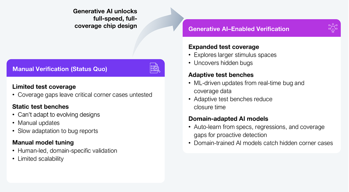
Source: HFS Research, 2025
GenAI transforms verification by addressing three longstanding challenges of the manual-verification status quo: limited test coverage, static test benches, and manual model tuning. GenAI creates synthetic data and generates diverse test cases. It explores larger stimulus spaces, closes coverage gaps, and reduces silicon escape bugs (a design error caught only during manufacturing). Adaptive testbench validation uses machine learning to analyze bug reports and coverage data, update test sequences, and track closure in real-time. AI models trained on specifications, regression data, and coverage gaps can expose hidden corner cases, reduce bias, and improve functional coverage without additional manual effort.
This combination of GenAI for synthetic data and diverse test case generation, adaptive testbench validation, and domain-adapted AI models shifts hardware verification from reactive debugging to proactive exploration, shortening regression cycles and enabling extensive, scalable validation as chip designs become progressively complex. As TCS demonstrated at DVCon, generative AI is moving rapidly from theory to practice, positioning itself as an enabler of next-generation chip design and verification.
HFS Research findings show that aligning partnerships across the semiconductor ecosystem and building trust are the key factors for the sector to scale up. Delays in technology roadmap implementation, IP development, and disconnects in co-innovation are three areas that need significant improvement. The semiconductor ecosystem must make targeted investments due to architectural and workflow complexities in domain-specific adaptations and establishing trust. Integrating AI with ecosystem workflows for autonomous decision-making will address these concerns by avoiding delays and uncovering insights that a human eye might miss.
As TCS demonstrated, scaling generative AI for verification promises smarter, faster, and more complete chip validation, where synthetic data and adaptive testbenches work in tandem to future-proof verification flows.
Register now for immediate access of HFS' research, data and forward looking trends.
Get Started


If you don't have an account, Register here |
Register now for immediate access of HFS' research, data and forward looking trends.
Get Started